
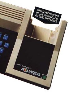
Cartridge / Extension bus
The cartridge bus on the back of Mattel Aquarius computer provides direct, unbuffered access to all of the address, data, and control lines, allowing the use of external peripherals (memory expansion, modems, and quick disk drives).
Extension Port
| Logic | TTL Compatible |
| Loading | ADR: 1 TTL load; DATA: 3 TTL loads; CTL: 1 TTL load |
| Port | 44 pin total (16 Adr, 8 Data, 3 Pwr & Gnd, 16 Control 1 Sound) |
Overview
| 1 | CSYNC | 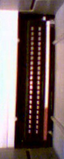 |
2 | SOUND |
| 3 | INT | 4 | BUSRQ | |
| 5 | RESET | 6 | M1 | |
| 7 | RFSH | 8 |  |
|
| 9 | A15 | 10 | A14 | |
| 11 | CE | 12 | A6 | |
| 13 | A5 | 14 | A7 | |
| 15 | A4 | 16 | A8 | |
| 17 | A3 | 18 | A9 | |
| 19 | A2 | 20 | A10 | |
| 21 | A1 | 22 | A11 | |
| 23 | A0 | 24 | A12 | |
| 25 | +5V | 26 | D0 | |
| 27 | D1 | 28 | D2 | |
| 29 | D3 | 30 | D4 | |
| 31 | D5 | 32 | D6 | |
| 33 | D7 | 34 | GND | |
| 35 | RD | 36 | A13 | |
| 37 | WR | 38 | MREQ | |
| 39 | NMI | 40 | WAIT | |
| 41 | HALT | 42 | BUSAK | |
| 43 | IORQ | 44 | GND |
Description
| PIN Nr | PIN Name | Symbol | Description |
| 1 | Composite Sync | CSYNC | Output, active low. Video synchronisation timing signal |
| 2 | Sound | SOUND | Input/Output, active high. External sound input or internal sound output. |
| 3 | Interrupt Request | INT | Input, active low. The INT signal is produced by I/O devices. |
| 4 | Bus Request | BUSRQ | Input, active low. It is used to allow other devices to take control over the process address bus, data bus and 3-state output control signals. |
| 5 | Reset | RESET | Input/Output, active low. When pull low, the Aquarius is reset. Interface may monitor or generate a reset. |
| 6 | Machines Cycle one | M1 | Input, active low. The INT signal is produced by I/O devices. |
| 7 | Refresh | RFSH | Output, active low. RFSH- indicates that a refresh address for memories is being held in the lower 7-bits of the address bus. |
| 8 | Clock | | Output, active high. Standard 3.579545MHz microprocessor clock signal. |
| 11 | Chip Enable | CE | Output, active low. Active when the computer addresses locations C000-CFFF |
| 23,21,19,17, 15,13,12,14, 16,18,20,22, 24,36,10,9 |
Address Bus | A0 - A15 | 3-State Output, active high. 16-bit address bus line. |
| 26 - 33 | Data Bus | D0 - D7 | 3-State Input/Output, active high. 8-bits, bidirectional data bus signals. |
| 25 | Power Supply | +5V | +5 Volts. |
| 35 | Memory Read | RD | 3-State output, active low. RD indicaties that the processor is requesting data from memory or an I/O device. |
| 37 | Memory Write | WR | 3-State output, active low. The Memory Write signal indicates that the processor data bus is holding valid data to be stored in the addressed memory or I/O device. |
| 38 | Memory Request | MREQ | 3-State output, active low. MREQ indicates that a valid address for a memory read or write operation is held in the address. |
| 39 | Non-Maskable Interrupt | NMI | Input, active low. NMI vectors the processor to subroutine at 0066. |
| 40 | Wait | WAIT | Input, active low. WAIT indicates to the processor that the memory or I/O devices being addressed are not ready for a data transfer. This pin has an internal 47k ohms pullup fore wire-0Red input. WAIT may also act as an output since it provides a 894.88KHz clock with 25% duty cycle. |
| 41 | Halt state | HALT | Output, active low. The processor willl execute NOP's while halted. |
| 42 | Bus Acknowledge | BUSAK | Output, active low. BUSAK indicates to the requesting device the processor address bus, databus and 3-state control bus signal have entered high impedance state. |
| 43 | Input/Output Request | IORQ | 3-State Output, active low. IORQ indicates that the lower half of the address bus holds a valid address for an I/O read or write operation. It is also generated concurrently with M1 during an interrupt acknowledge cycle to indicate that an interrupt response vector can be placed on the data bus. |
| 34,44 | Power GND | GND | System electrical ground. |